ASML Set to Soar: Unleashing Growth from US, Japan, and Korea's Chip Boom

By Viga Liu
Key Takeaways
· EUV Monopoly: ASML holds a 100% market share in EUV lithography, essential for sub-5nm chip production, ensuring its market dominance.
· Regional Growth: Strong demand from the US, Japan, and Korea drives ASML's growth, with significant investments and strategic shifts in these regions.
· Technological Edge: Advancements in High-NA EUV technology position ASML at the forefront of chip miniaturization.
· Valuation: ASML's fair value estimated at $801-$978 per share, reflecting its critical role in advanced semiconductor manufacturing.
Company Overview
ASML Holding N.V., headquartered in Veldhoven, Netherlands, leads the semiconductor sector by specializing in advanced photolithography equipment. This equipment is crucial for creating microchips, as it precisely etches patterns onto silicon wafers. ASML's innovation in EUV (Extreme Ultraviolet) lithography technology has established it as the sole provider of systems for manufacturing the latest semiconductor chips, giving it a distinct advantage worldwide.
Industry Position:
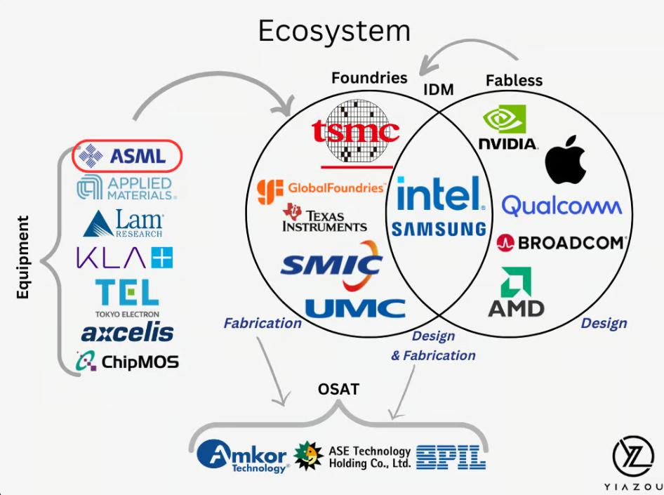
Source: Yiazou
Monopolistic Technology: ASML holds a monopoly in the EUV lithography market, with no competitors able to replicate its advanced technology, production scale, or comprehensive support network. As of 2024, ASML holds a 100% market share in EUV lithography systems, a clear indicator of its indispensable role in the semiconductor industry. Every cutting-edge semiconductor node below 5nm relies exclusively on ASML's equipment, solidifying its critical position in enabling next-generation chip manufacturing.
Irreplaceability: The EUV lithography market is characterized by exceptionally high barriers to entry. Developing systems like ASML's High-NA EUV requires decades of expertise, billions in R&D investment, and a highly specialized global supply chain. These factors, combined with the sheer complexity and cost of technology, make it virtually impossible for new entrants to compete, ensuring ASML's continued dominance in this critical niche.
Comparative Performance: Unlike other semiconductor equipment manufacturers, ASML's business model is less susceptible to market fluctuations. This resilience stems from the irreplaceable nature of its EUV technology, which is essential for technological progress rather than mere capacity expansion. As a result, ASML benefits from a more predictable and stable revenue stream compared to its peers.
Semiconductor Manufacturing Process
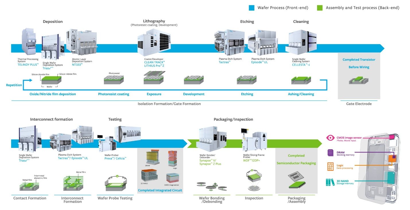
Source: Tokyo Electron Limited
In semiconductor manufacturing, lithography is a pivotal step in constructing intricate microelectronic circuits on silicon substrates, spanning processes like wafer preparation, patterning, doping, metallization, testing, and packaging. Production begins with wafer preparation, followed by layered processes to build the chip’s 3D structure. Lithography, critical for patterning, relies on ASML’s DUV and EUV systems.
Key Aspects of Lithography:
1. Patterning Precision: Lithography machines project circuit patterns onto photoresist with high accuracy. Exposure triggers chemical changes, allowing development to remove unwanted sections, leaving precise patterns that determine chip performance, power efficiency, and size.
2. Multi-Layer Patterning: essential for modern chips, which can have dozens of patterned layers. EUV lithography enables the creation of smaller features required for advanced nodes like 5nm and 3nm, while DUV lithography handles larger nodes and less critical layers. EUV can also reduce the complexity of multi-patterning compared to relying solely on DUV for advanced nodes.
3. Efficiency and Yield: ASML’s lithography machines improve accuracy, efficiency, and yield through techniques like multiple patterning and self-alignment, reducing defects.
4. Technological Advancements: ASML’s EUV technology, including High-NA EUV systems, drives the industry’s push for smaller feature sizes, enabling more efficient, high-performance chips.
5. Cost and Complexity: Lithography machines are among the most expensive and complex in semiconductor production. EUV systems, despite high costs, are essential for advanced node manufacturing.
In summary, lithography is a complex and critical step in semiconductor manufacturing, directly influencing chip characteristics, performance, and competitiveness. ASML’s leadership in lithography technology is indispensable to advancing the industry.
Key Technologies
DUV (Deep Ultraviolet) Lithography:
DUV lithography, a workhorse of semiconductor manufacturing, uses ultraviolet light with wavelengths of 248 nm or 193 nm, generated by excimer lasers, to create intricate circuit patterns on silicon wafers. This process involves projecting light through a mask (also known as a photomask) containing the desired circuit pattern onto a wafer coated with a light-sensitive photoresist. The DUV light passes through the transparent portions of the mask and is precisely focused onto the wafer by refractive lenses. When the light hits the photoresist, it causes a chemical reaction, and depending on the type of photoresist being used, either the exposed or unexposed areas are then removed, leaving the desired circuit pattern. This whole process is akin to shining a UV flashlight through a stencil onto photosensitive paper, selectively changing the paper's properties, and then washing away either the exposed or unexposed areas to reveal the stencil's pattern.
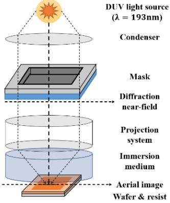
Source: Optics Express
· Applications:
o Node Size: Primarily used for 10nm and above, but through multi-patterning techniques (e.g., double patterning), it also supports smaller nodes.
o Industry Use: Widely employed in consumer electronics, automotive, IoT, and more.
· Key Clients:
1. TSMC: A major ASML customer, with hundreds of DUV systems. TSMC continues to invest in DUV for mature nodes despite its focus on EUV.
2. Samsung: Utilizes hundreds of DUV systems for DRAM, NAND, and logic chips, maintaining steady demand for mature nodes.
3. Intel: Employs DUV systems for CPUs, GPUs, and other products, with ongoing investments under its IDM 2.0 strategy.
4. GlobalFoundries: Focuses on mature nodes (e.g., 14/12nm), ensuring stable DUV demand.
5. SK Hynix: Relies on DUV for memory production, with demand driven by trends like HBM.
6. Micron: Adjusts DUV procurement based on memory market cycles.
7. Japanese Firms (e.g., Toshiba, Sony): Maintain steady DUV usage for specialized markets.
8. Chinese Manufacturers (e.g., SMIC): Continue to seek DUV systems to support domestic semiconductor production, despite export restrictions.
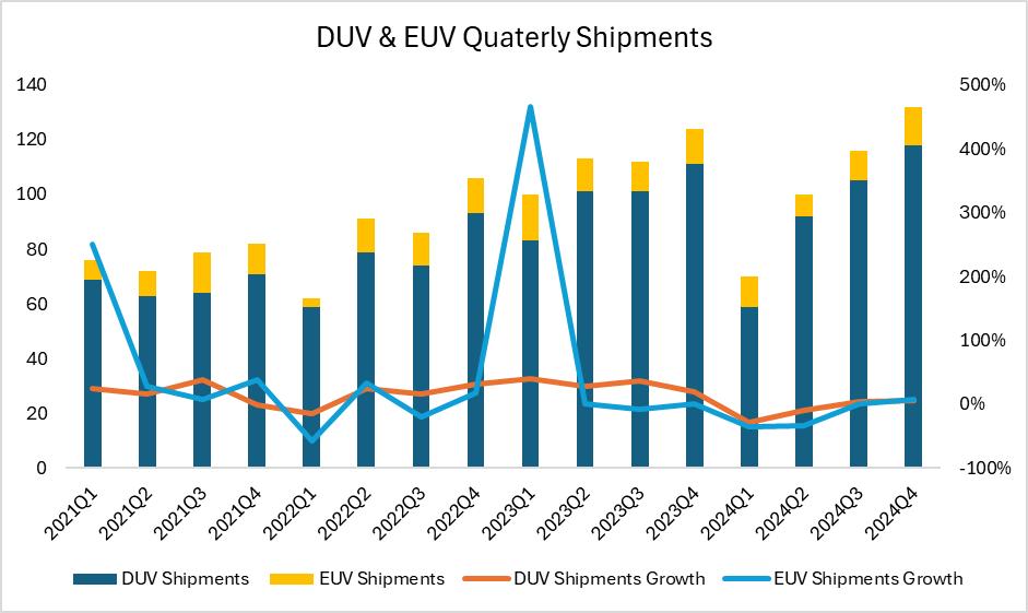
· Quarterly Shipments: In Q4 2024, ASML shipped 118 DUV systems, including immersion and KrF models.
EUV(Extreme ultraviolet) Lithography:
EUV lithography is a cutting-edge technology used in the semiconductor industry to manufacture integrated circuits with nanometer-scale resolution4. The process begins with a high-power laser that strikes droplets of tin in a vacuum chamber, creating a plasma that emits EUV light at a wavelength of approximately 13.5 nm. This light is then collected and directed by ultra-flat, multi-layered mirrors through a reflective photomask, which imprints the desired circuit pattern onto a substrate covered by a photosensitive material called photoresist. The areas exposed to the EUV light undergo a chemical change and are subsequently etched, allowing for the deposition of new materials to form the microchip's components. This process can be repeated multiple times with different masks to create complex, multilayered circuits on a single wafer.
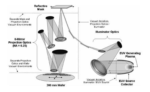
Source: The International Society of Optical Engineering
· Applications:
o Node Size: Essential for 5nm and below, enabling high-density, high-performance chips.
o Industry Use: Critical for HPC, AI, 5G, and advanced memory (e.g., HBM).
· Key Clients:
1. TSMC: A leading EUV adopter, with dozens of systems for 5nm, 3nm, and beyond.
2. Samsung: Invests heavily in EUV to maintain competitiveness in logic and memory.
3. Intel: Deploys EUV systems under its IDM 2.0 strategy, with plans for High-NA EUV adoption.
4. Other IDMs/Foundries: Limited EUV adoption currently, but potential for growth as technology advances.
· Quarterly Shipments: In Q4 2024, ASML shipped 14 EUV system. High-NA EUV shipments remain limited but are expected to grow as the technology matures.
Source: ASML, Tradingkey.com
High-NA EUV Progress:
· Breakthroughs: ASML’s High-NA EUV systems (NA=0.55) enhance resolution and enable single-exposure patterning for 2nm and beyond, improving efficiency and yield.
· Clients: Intel has received the first High-NA EUV systems, with TSMC and Samsung expected to follow.
· Production & Delivery: ASML plans to scale High-NA EUV production, with mass deliveries expected in 2025–2026.
Growth Driver
According to ASML’s Q4 2024 financial report, both DUV and EUV lithography machine shipments experienced great growth, reflecting a notable increase in market demand.
AI Market Expansion:
During the post-earnings conference call, CEO Christophe Fouquet highlighted that the expansion of AI applications is a key driver of this demand. The growing need for high-performance computing chips in AI has fueled the demand for ASML’s advanced lithography technologies. As AI applications expand into areas such as cloud computing, data centers, and autonomous driving, ASML’s customers, including TSMC and Samsung, have increased their procurement of EUV equipment to meet the demand for high-performance chips in these sectors.
Technological Advancements:
ASML’s development of High-NA EUV technology is expected to further drive miniaturization and efficiency of chip manufacturing. ASML has already begun delivering High-NA EUV systems to customers. While conventional EUV lithography systems operate with a numerical aperture of 0.33, High-NA EUV increases this to 0.55. This advancement enables a 1.7x reduction in chip size and a 2.8x increase in transistor density. With an increased numerical aperture, High-NA EUV systems enable more precise patterning of smaller circuit features, which is critical for meeting the demands of high-performance computing applications such as AI.
Global Semiconductor Demand:
ASML noted that its order and revenue growth aligns with the expansion of the global semiconductor market, particularly in data centers and AI accelerators. For the full year of 2024, ASML reported net sales of €28.3 billion, with Q4 net sales reaching €9.3 billion, underscoring the strong growth in market demand.
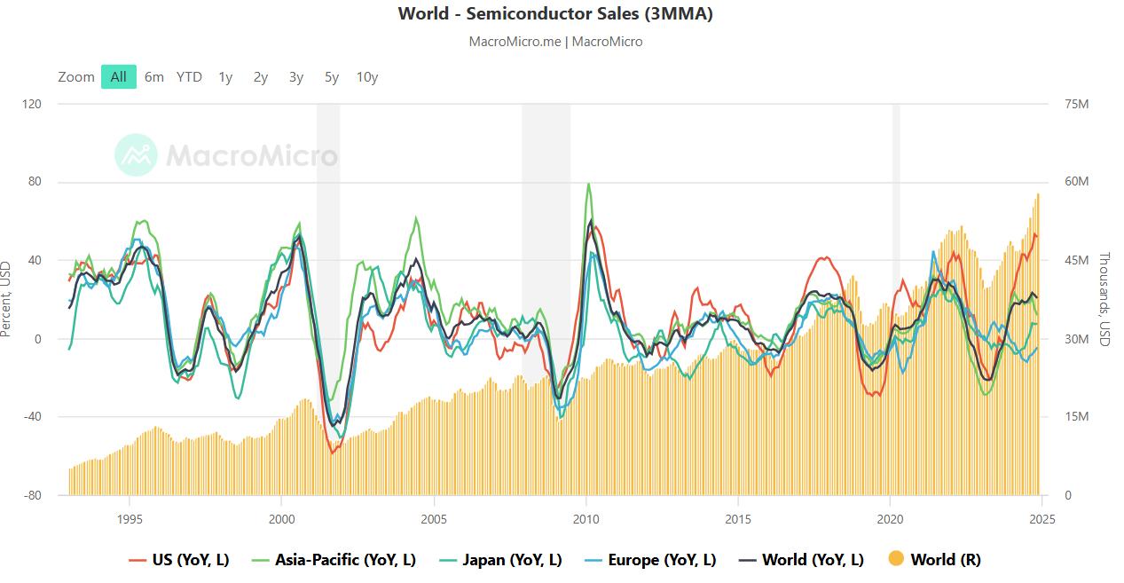
Source: MacroMicro
End Use
The semiconductor market’s end-use applications and segments are projected to exhibit the following trends in the coming years.
Source: WSTS
Source: ASML, Tradingkey.com
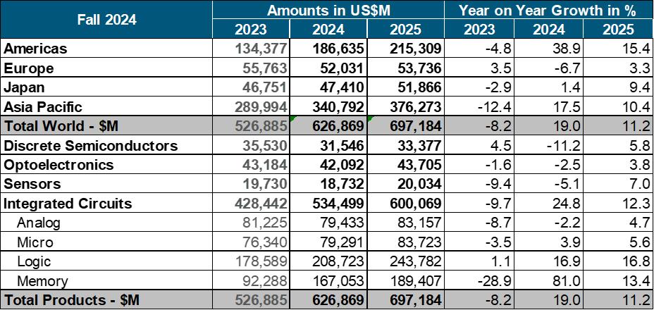
Memory:
In 2024, the memory market achieved an impressive growth rate of 81.0%, driven primarily by demand for NAND flash and DRAM, particularly in applications such as data centers, consumer electronics, and mobile devices. For instance, data centers require substantial NAND flash for data storage, while DRAM is essential for accelerating data processing and computational tasks. In 2025, the memory market is expected to grow by 13%, reaching a market size of approximately $190 billion. Although this growth rate is lower than that of 2024, the market is entering a period of relatively stable demand.
HBM Growth:
The demand for High Bandwidth Memory (HBM) is rising alongside the expansion of AI applications and high-performance computing needs. HBM offers higher bandwidth and lower power consumption, making it ideal for AI accelerators and high-performance computing systems. Its market share is expected to continue growing, further driving the overall expansion of the memory market.
Logic:
The logic chip market is projected to grow by 16.8% in 2025, similar to its growth rate in 2024, making it a massive segment with a market value exceeding $240 billion. The demand for logic chips is fueled by the need for more powerful and efficient chips, particularly in AI, cloud computing, 5G communications, IoT, autonomous driving, edge computing, and high-end gaming and entertainment.
AI and Cloud Computing Driving Growth:
The advancement of AI and the increasing demand for cloud computing are key factors propelling the logic chip market. For example, the demand for high-performance computing chips, GPUs (Graphics Processing Units), and TPUs (Tensor Processing Units) used in AI training and inference continues to surge. These chips play a central role in data centers and cloud services while also enabling localized AI processing on edge devices. This demand not only drives the growth of the logic market but also accelerates technological advancements in semiconductor nodes, such as the transition from 7nm to 5nm, 3nm, and beyond, fostering investments in EUV technologies by companies like ASML.
Regional Revenue Trend
Source: ASML
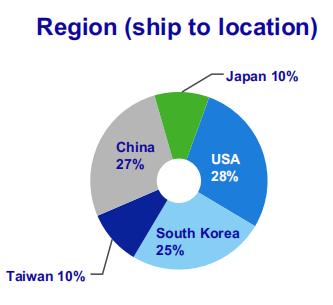
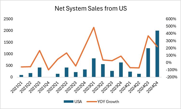
Dominance of the U.S. Market:
The U.S. market has become ASML’s largest revenue source. According to WSTS data, the memory chip market grew by 81% in 2024, aligning with a 38.9% revenue increase in the Americas. However, the logic chip market is expected to perform even stronger in 2025. IDC’s market research indicates that the ongoing expansion of AI and cloud computing markets will drive the growth of the U.S. logic chip market. As the U.S. continues to increase its share in the semiconductor market, particularly in logic chips, ASML’s revenue in the region is expected to grow accordingly.
Source: ASML, Tradingkey.com
Shift from Taiwan to the U.S.:
In Q4 2024, a notable trend emerged where part of Taiwan’s semiconductor revenue shifted to the U.S. This change is largely driven by TSMC’s expansion strategy in the U.S. TSMC’s first fab in Arizona has made significant progress and is expected to begin mass production of 3nm chips in Q1 2025. A second fab, focusing on more advanced 2nm chips, is projected to start production in 2028. Despite challenges such as labor shortages and high costs, these projects underscore TSMC’s long-term commitment to the U.S. market.
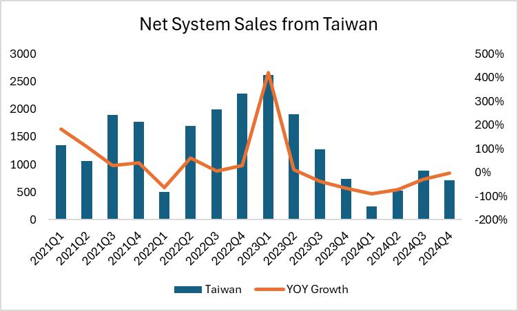
Source: ASML, Tradingkey.com
South Korea:
In Q4 2024, ASML’s revenue from South Korea increased, primarily driven by the strong performance of the memory chip market. Major South Korean semiconductor manufacturers like Samsung and SK Hynix are predominantly focused on memory chip production, leading to this revenue growth. However, global market trends indicate a shift towards logic chips, with WSTS forecasting a logic chip market growth of over 17% in 2025, compared to the relatively slower growth in the memory segment. This shift reflects the increasing demand for AI, cloud computing, and other applications, which is expected to drive rapid growth in the logic chip market in the future. While this transition is on the horizon, the 2024 Q4 revenue increase from South Korea was not directly influenced by this trend but rather by the current strength in memory chip demand.
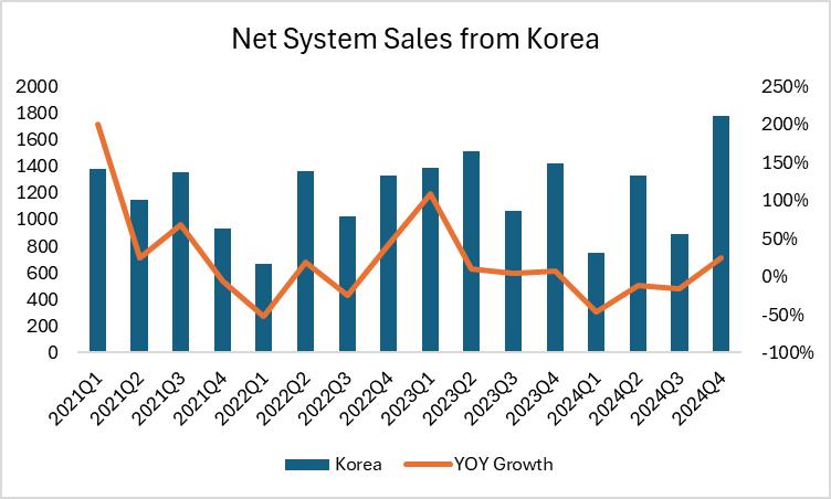
Source: ASML, Tradingkey.com
Japan’s Major Moves:
The Japanese government is making significant strides in semiconductor manufacturing through initiatives like the Rapidus project, which includes an investment plan exceeding JPY 10 trillion. Rapidus aims to begin trial production of 2nm chips in 2025, signaling Japan’s ambition to re-emerge as a key player in the semiconductor industry. Japan’s semiconductor sector is also accelerating its manufacturing capabilities through several other projects, such as Micron’s plan to introduce EUV lithography at its Hiroshima plant starting in 2026, TSMC’s expected introduction of EUV technology at its second Kumamoto fab in 2027, and the establishment of an EUV R&D base in collaboration with Intel and Japan’s National Institute of Advanced Industrial Science and Technology (AIST).
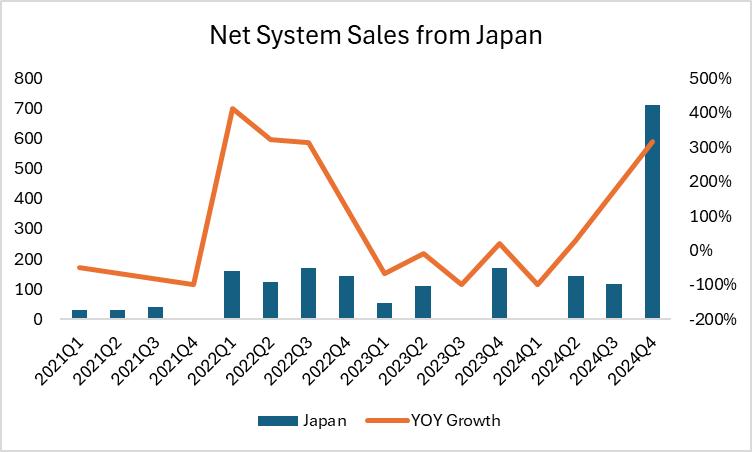
Source: ASML, Tradingkey.com
Decline in China’s Revenue:
China’s revenue share dropped from over 40% two years ago to 27% in 2024. This decline is mainly due to the peak in domestic wafer fab construction in 2022 and 2023, leading to a period of capacity digestion. According to TrendForce, after a period of rapid expansion, China’s semiconductor market entered a phase of capacity consolidation and adjustment in 2024, impacting short-term revenue. Chinese semiconductor manufacturers are now focused on adjusting production to align with market demand and avoid wasting excess capacity.
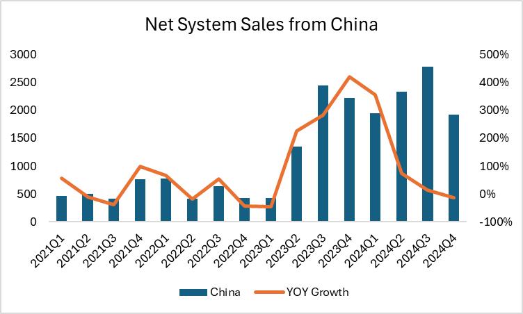
Source: ASML, Tradingkey.com
Financials:
ASML's revenue growth has been robust, with year-on-year increases of 33% in 2021, 14% in 2022, 30% in 2023, and 3% in 2024 fueled by the semiconductor demand spike due to the global push towards digital transformation, the 5G roll-out, and AI expansion. In 2024, ASML's stock plummeted from $1000 to below $700 primarily due to disappointing Q3 earnings with lower-than-expected net bookings and a significant cut in the 2025 sales forecast. Additionally, market softness in non-AI chip sectors, delays in orders from major clients, and concerns over export restrictions to China contributed to the sharp decline. The situation for ASML has improved a lot due to the growth in several key areas discussed above.
Net Sales: ASML reported Q4 net sales of €9.3 billion, which is a 28% increase year-over-year (YoY). This strong growth reflects the high demand for ASML's EUV and DUV systems.
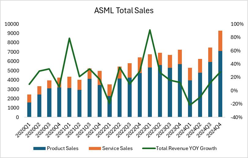
Source: ASML, Tradingkey.com
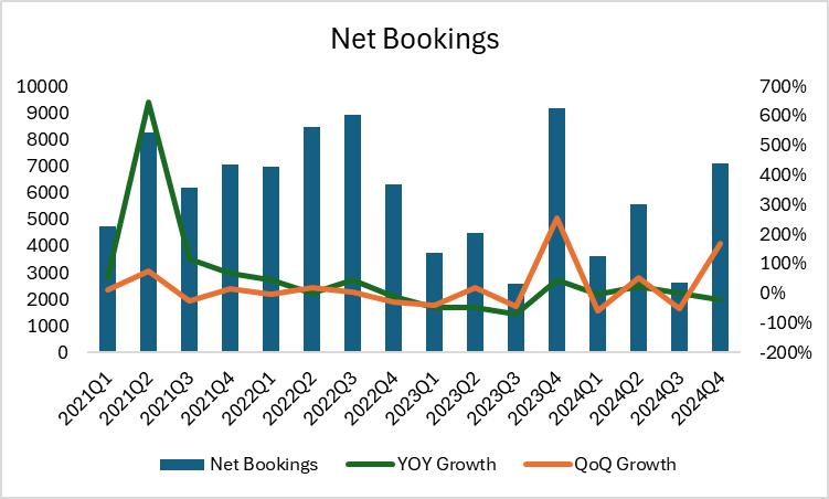
Net Bookings: Net bookings provide a forward-looking view of a company's financial health, as a critical indicator of a company's future revenue potential, especially in industries like semiconductor equipment manufacturing where ASML operates. Net bookings for Q4 stood at €7.1 billion, with €3.0 billion from EUV systems, 169% increase from Q3, showing a significant increase from the previous quarter, suggesting strong future revenue potential.
Source: ASML, Tradingkey.com
In summary, ASML's Q4 2024 performance was marked by substantial growth in net sales, service sales, and net bookings, highlighting the company's strong market position and the increasing demand for its advanced semiconductor manufacturing solutions.
Valuation
We expect ASML’s fair value in the range of $801 to $978 per share. This valuation reflects ASML’s leadership in lithography technology and its critical role in enabling advancements in AI, cloud computing, and high-performance chips.
Key Assumptions
· Revenue Growth: Projected growth of 15% in 2025, 13% in 2026, and 10% in 2027, driven by strong demand for EUV and High-NA EUV systems.
· EBIT Margin: 40%, reflecting ASML’s pricing power and operational efficiency.
· Terminal Growth Rate: 3%, supported by the long-term growth trajectory of the semiconductor industry.
· WACC: 6.5%, reflecting ASML’s strong market position and lower risk profile.
ASML’s strong growth prospects and pivotal role in the semiconductor industry support a target price range of $801 to $978 per share, with upside potential of 10%-30%, driven by increasing demand for advanced lithography solutions. The target price range is derived from a sensitivity analysis varying WACC (6.0%–7.0%) and perpetual growth rate (2.5%–3.5%), accounting for uncertainties in long-term industry growth.